End of YouTube
Clickbait

AI summaries of any CCed video in seconds. Know the key points, defeat clickbait, and learn 10x faster.

https://www.youtube.com
YouTube Video
U

YouTube Video zr8nLCnX1jk

Unknown Channel

52 minutes ago

YouTube Video
U

YouTube Video zoYY3JdPQ3Q

Unknown Channel

13 days ago

2,000+
Summaries generated
2.6s
Median generation time
10+
Summary languages
1,900+
Videos summarized

Your Day, Hijacked by Fluff

Time is your most valuable asset. Here’s how YouTube spends it for you.

  • 9:00 - 9:25
    A 25-minute tutorial where the 2-minute solution is buried at the end.


  • 14:30 - 14:45
    A 15-minute 'review' that pushes affiliate links instead of giving a clear answer in 1 sec.


  • 19:45 - 20:20
    A 'quick' video that leads to a 35-minute rabbit hole of irrelevant content.
Total Daily Loss
75
min/day
A full work week, gone.
40+
hrs/month

Why do I have to watch half a video just to know if it's actually useful?

— Anyone who values their time

There's a smarter way...

Know the contentbefore you watch

1.

Click the PeekaTube Icon for an Instant Summary

On any YouTube video that has captions, simply click the PeekaTube icon (PeekaTube Icon). An AI-powered summary will be generated in seconds.
2.

See What Viewers Think, Too

Every summary folds in the video's top comments alongside the transcript. You catch the reception, corrections, and consensus without scrolling the comment section yourself.
3.

Learn Faster or Move On

Instantly decide if the video is worth your time. Absorb the insights you need, or confidently walk away to find better content.
Try the Better Way(Free!)

View & Exportin One Place

Transcripts • Summaries
en
3.27s
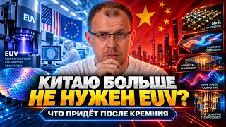
Imagine a situation: in a few years, China releases a processor that can not be manufactured on modern ASML machines. Not because the Chinese somehow copied EUV lithography, but because they simply do n't need it anymore. Instead of silicon, there are two-dimensional materials only a few atoms thick; instead of conventional transistors, there are electron waves. And for storing information, instead of thousands or millions of electrons, literally just one is used. It sounds like science fiction, but research into each of these areas already exists today. And the most interesting part is that a huge portion of it is currently emerging specifically in China. Hello everyone! My name is Dmitry from InXnon Lab. Today, we 'll try to figure out if humanity is truly approaching the limit of silicon processors. What could replace them? Why is everyone suddenly talking about gallium oxide, graphene, two-dimensional transistors, and quantum memory? And the main question: could China not just catch up to the West in modern microelectronics, but simply leapfrog over existing technology? And what is actually wrong with silicon? Practically all modern electronics are built around one rather simple idea: if you need to increase performance, you shrink the transistors. You shrink the transistors, and more elements fit into the same area, resulting in a more powerful processor. And that is how the industry has lived for decades. But the problem is that today the dimensions of individual transistor elements are already measured in just a few nanometers, while a silicon atom is about two-tenths of a nanometer in size. In other words, we are gradually approaching a scale where what follows is no longer familiar engineering, but quantum physics. Electrons begin to tunnel through barriers that are too thin, leakage currents increase, heat dissipation becomes more difficult, and production becomes increasingly expensive. And the problem is n't just about physics. Each new generation of lithography requires incredibly complex equipment. A modern EUV machine consists of tens of thousands of components and costs hundreds of millions of dollars. And a factory for the most advanced chips now costs tens of billions. It turns out to be a paradox: the transistor is getting smaller, but the cost of the ability to make it smaller is growing almost exponentially. That is why the industry 's main question is gradually changing. Previously, they asked: how do we make a silicon transistor smaller? Now, they are asking more and more often : why do we even have to keep using silicon? And this is where the first candidate appears. Is gallium oxide the new silicon? If you follow tech news, you 've probably come across the name 'gallium oxide'. Sometimes it is already being called a material capable of replacing silicon. There is just one small problem here. That is not entirely true. Gallium oxide does indeed possess a very wide bandgap, and it is capable of withstanding significantly stronger electric fields than conventional silicon. This unique set of characteristics makes it extremely interesting for the field of power electronics. Electric vehicles, power supplies, industrial converters, energy, data centers — that is, areas where you need to manage huge amounts of power with minimal losses. And China is currently developing this direction very actively. In twenty twenty six, Chinese companies already reported the production of large six- and eight-inch gallium oxide wafers. And the transition to larger wafers is already one of the most important signs that the technology is trying to move from the laboratory to industry. But here an important point arises: your next Ryzen will most likely not be made of gallium oxide. For standard high-performance CPUs, this material has enough problems of its own. For example, it dissipates heat quite poorly. Therefore, it is more accurate to say this: gallium oxide will not replace silicon, but it is starting to take over specific tasks from silicon. And this is, perhaps, the main principle of the electronics of the future. There will not be one single material that replaces silicon. There will be many different materials, each for its own specific task. But if we talk directly about processor transistors, things get much more interesting here. A processor only a few atoms thick. Here is a standard silicon transistor. Now imagine that its active layer is literally only a few atoms thick. That is precisely why so much attention is currently being paid to so-called two-dimensional materials. One of the most well-known is molybdenum disulfide. Its layer can be practically atomically thin. And in theory, this is very convenient because such a thin channel is significantly easier to control with an electric field, which means that transistors can potentially continue to be shrunk even where silicon is already starting to experience serious problems. And here, China recently showed a very interesting result. Researchers from Tsinghua University have created a MOS transistor with a physical gate length of less than one nanometer. Moreover, it was n't limited to just one beautiful device under a microscope. The scientists demonstrated arrays of transistors and then assembled them into simple NAND and NOR logic gates. And these are literally the building blocks of any processor. At first glance, it seems: well, that 's it, here is the processor of the future. But there is one figure that is usually not put in the headline. For the smallest transistors, the yield of working devices is approximately fifteen percent. That is, conditionally, out of one hundred manufactured devices, fifteen work properly. But a modern processor needs billions, and it is desirable that almost all of them work. This is the huge gap between "scientists have created a transistor smaller than a nanometer" and TSMC producing a billion such transistors on every chip. A laboratory record is the beginning of the journey, not the end. But there is an even more radical option. What if, instead of shrinking transistors, we abandon the conventional method of computing altogether? And before we continue, just a few seconds. Xenon Lab. We are trying to create an independent scientific and technological project. If you really enjoy what we do, you can support us on Boosty or Patreon. You can subscribe to our channel, or simply leave a donation. This will help us make more episodes like this, and spend more time on research, graphics, filming, and editing. Thank you for your support. The link to Boosty and Patreon is in the channel header. Thanks to everyone who is already supporting the project. And we return to silicon. What if we computed not with electrons, but with waves? This is where real science fiction begins. A modern processor works something like this: there is a transistor, and it either lets current through or it does n't. We get a zero or a one. Billions of these tiny electronic switches add up to complex computations. But in nature, there is actually a huge number of other ways to transmit information. For example, consider waves. A wave has amplitude, frequency, and phase. When two waves meet, they can either amplify each other, creating a stronger signal, or they can completely cancel each other out. In other words, the fundamental physics of interference is already performing a complex mathematical operation, which is precisely why scientists are actively researching the potential of so-called wave-based computing. Moreover, these waves can be completely different in nature: they might be light, acoustic, spin, electromagnetic, or even collective electron waves. Back in 2026, a team of Chinese researchers demonstrated a truly unusual device based on graphene. Under certain specific conditions, the electrons and holes in graphene begin to behave collectively, acting almost like a liquid. Fascinatingly, special waves can actually propagate through such an electron liquid. The researchers managed to create a device that can control the propagation of such a wave, allowing it to pass through or reflecting it. In essence, this results in a kind of wave transistor. No, you ca n't run Windows on it yet, and it 's too early for a calculator, too. But the idea itself is what matters. We try to make computations faster by forcing billions of transistors to switch billions of times per second. And nature can sometimes perform a mathematical operation simply because two waves met each other. For some tasks, this could potentially be much more efficient, especially for artificial intelligence, signal processing, and matrix calculations. But the processor is only half the problem, because a modern computer spends a huge amount of energy not on calculations at all. One bit - one electron. The big problem with modern computing is called quite simply: data constantly needs to be moved somewhere. From memory to the processor, from the processor back, from HBM to GPU, from one accelerator to another, and this requires energy. Moreover, with the growth of artificial intelligence, the problem is becoming increasingly serious, and therefore new memory can change computers no less than a new processor. In the summer of 2026, researchers from Fudan University presented a groundbreaking experimental memory device in which literally just 1 single electron is enough to store 1 bit of information. For comparison, in traditional electronics, a huge number of electrons are used to reliably determine the state, whereas here, the state of a single electron is being changed instead. Moreover, the device operates at room temperature. And this is already extremely interesting, because if such technologies can ever be scaled, the power consumption of memory could potentially be reduced very significantly. But here, the marketing confusion begins again. Under headlines like "Quantum Memory," completely different technologies can be hidden. One type of electronic memory is one thing, but true memory for quantum computers is something else entirely. There, you need to store not an ordinary zero or one, but a quantum state, for example, the state of a photon or a qubit. And China is simultaneously working actively in this area as well. So, we are arriving at a rather unexpected picture. The computer of the future might not consist of just one type of electronics at all. The processor is one material, the memory is another, the power component is a third. Data transmission via light, specialized computing via waves, and right next to it, a separate quantum module. And now the most uncomfortable question arises: can China bypass the sanctions? Because this is exactly where this whole story becomes much more interesting than ordinary science. Today, the US and its allies are trying to restrict China 's access to the most advanced semiconductor manufacturing technologies. The most well-known example is EUV lithography. ASML remains the only company capable of mass-producing such systems, and China does not officially receive them. From this arises a very tempting idea: if China can not quickly catch up with the West in traditional silicon technologies, maybe it will simply create a technology that does n't need EUV at all? And theoretically, yes, it is possible. If a new architecture requires less aggressive lithography, if part of the computation is performed in memory, or if 3D structures, chiplets, photonics, new materials, or wave accelerators are used, then the heavy dependence on a specific process node can indeed decrease significantly. But there is one important point: new physics does not cancel out manufacturing. A two-dimensional transistor still needs to be manufactured, the material needs to be grown. It involves controlling microscopic defects, applying precise contacts, forming insulation, and creating conductors. Then, we are producing billions of elements, testing them, packaging them, and finally, designing the architecture and software for all of this. Therefore, an article in Nature does not replace a TSMC factory, and a new material does not eliminate technological sanctions overnight. But it can change the rules of the game, because a sanction is especially effective when there is one main technological path. For example, do you want the best processor? You need the best manufacturing process, you need EUV, you need specific equipment. But if there are ten paths, then controlling all the bottlenecks becomes much more difficult. What will actually come after silicon? And now let 's try to make a forecast. Trend number one. Silicon is not going anywhere. It is too cheap, too well-studied. A gigantic industry has been built around it. Therefore, you should n't expect that in five years all factories will throw away silicon and switch to graphene. Trend number two. Silicon will cease to be the universal material for everything. Power electronics will increasingly use silicon carbide, gallium nitride, and possibly gallium oxide. Two-dimensional materials may appear for individual transistors. Communication between chips will gradually shift to photonics. Trend number three. Computing is set to become increasingly specialized. Today, the CPU tries to be a universal processor, but AI has already shown just how effective specialized accelerators can be. In the near future, individual computing blocks may rely on completely different physical principles: some will use transistors, others will utilize light, others will leverage memory, and still others will harness waves. Trend number four. The main race will no longer be the race for nanometers. We are quite accustomed to comparing seven nanometers, five, or even two, but in a few generations, this figure may cease to be the primary indicator of technological leadership. That is because the much more important question will be: how many useful computations a system performs per watt of energy. And this is where countries that are currently lagging behind in classical lithography really have a chance to change the balance of power. Is the silicon era really coming to an end? Actually, both yes and no. Silicon will remain the foundation of electronics for a long time. It wo n't disappear tomorrow, it wo n't disappear in five years, and perhaps it wo n't disappear in twenty either. But the era when practically any performance problem could be solved by simply shrinking the silicon transistor is indeed coming to an end. And now, a much more interesting period is beginning. Instead of one technology, dozens are emerging. Gallium oxide, silicon carbide, two-dimensional materials, photonics, in-memory computing, electronic and spin waves, quantum devices. And that is precisely why I would keep a close eye on what is happening right now in Chinese laboratories. Not because China will release a processor tomorrow that will overtake Nvidia or AMD, but because a technological lag sometimes forces you to look for a path that others simply have n't taken yet. And here remains the main, critical question : what is truly more dangerous for a leader? Is it a competitor who is actively trying to catch up with you, or is it a competitor who has completely stopped running on your track altogether? And now, a question for you. What do you think will really be the next big stage after silicon? Are we looking at two-dimensional transistors, photonics, in-memory computing, or perhaps quantum technologies? Or, do you think silicon will continue to bury all of its would-be killers for another thirty years? Write in the comments. This was Dmitry from Xenon Lab. Subscribe, like, and hit the bell. See you in the next video.
  1. TL;DR — As traditional silicon scaling nears its physical and economic limits, researchers—particularly in China—are exploring alternative materials and paradigms like 2D transistors, wave-based computing, and single-electron memory. While these breakthroughs won't replace silicon overnight, they could eventually bypass the need for advanced EUV lithography and reshape global technological leadership.

  2. Key Points

    • 01:33 — Silicon is hitting fundamental limits in physics (quantum tunneling, high heat, and leakage currents) and economics, where shrinking transistors requires exponentially more expensive lithography equipment.
    • 02:34 — Gallium oxide emerges for power electronics (handling high power with low losses), though it is not suitable for high-performance CPUs due to poor heat dissipation.
    • 04:36 — Two-dimensional materials (like molybdenum disulfide) enable atomically thin channels; Chinese researchers have successfully built sub-nanometer ga

From Chaos to Clarity

Drag the slider to see the difference. Stop watching, start understanding.

The Old Way

The 25-Minute Gamble

Hunting for the answer
Skipping ads and fluff
Losing focus to clickbait

The PeekaTube Way

The 3-Second Summary

Get key takeaways instantly
Access relevant timestamps
Achieve zero distractions

Stop Wasting Time on Clickbait.

Peekatube gives you instant AI summaries of any YouTube video, so you know what it’s about before you click

25% Off Beta

Pro Plan

Unlimited AI summaries for any YouTube video

$5.99/month
  • Lightning-fast summaries for any CCed Youtube video
  • Unlimited video summaries
  • Also includes:
  • Early feature access
  • One-click summary & transcript export
  • Priority support
  • Chrome extension
  • or $44.99/year (save 25%)

Frequently Asked Questions

Everything you need to know about PeekaTube

How does PeekaTube work?
It's simple. You provide a YouTube link, and our AI reads the video's captions (CC) or transcript, analyzes the key points, and generates a well-structured summary. PeekaTube also fetches YouTube comments to give you additional context — like viewer corrections, expert opinions, and community reactions — that the video alone doesn't cover.
Does it only work with videos that have CC subtitles?
Currently, yes. The quality of our summaries depends heavily on the accuracy of video captions. However, support for videos without subtitles is in development. If you really need this feature, you can
What types of videos work best for summaries?
PeekaTube excels at processing content centered around 'dialogue,' such as: educational lectures, technical tutorials, interviews, documentaries, and news reports. Basically, as long as a video has subtitles, our AI can analyze it.
How accurate are the summaries?
Our AI is designed to capture the core ideas and structure of videos with high accuracy. However, think of it as a smart 'viewing guide' rather than a complete replacement for watching. It's perfect for determining if a video is worth your time and quickly grasping its key concepts.
What languages are supported?
PeekaTube can not only process multiple source languages but also translate summaries into your preferred language. For example, you can generate a Chinese summary for a Japanese video. Currently supported output languages include: Chinese, English, Japanese, Korean, Spanish, French, German, Italian, Portuguese, and more.
Can the processing speed be faster?
I'm constantly working to optimize speed! The current processing time includes necessary steps to ensure service stability. To prevent YouTube from blocking our IP, the backend uses proxies to ensure PeekaTube continues running reliably for you. While this adds a few seconds to processing time, it's a crucial trade-off for maintaining uninterrupted service. My goal is to continuously improve processing speed without sacrificing stability.
Who is this tool for?
PeekaTube is for anyone who values their time: - Students: Research and course review - Professionals: Stay updated on industry trends and tutorials - Lifelong learners: Explore new knowledge without wasting time
What are the latest features and future plans?
We've launched the Chrome extension — Pro users can now use PeekaTube directly on YouTube pages! We've also added YouTube comment analysis, which fetches viewer comments to give you a fuller picture of the video beyond just the transcript. Coming next: support for videos without subtitles is actively being developed. Your support is the biggest motivation for making new features available sooner!

Have more questions?

We're happy to answer any questions you might have